- 您现在的位置:买卖IC网 > Sheet目录3878 > PIC18F4410T-I/ML (Microchip Technology)IC MCU FLASH 8KX16 44QFN
PIC18F2X1X/4X1X
DS39636D-page 142
2009 Microchip Technology Inc.
15.4.2
PWM DUTY CYCLE
The PWM duty cycle is specified by writing to the
CCPR1L register and to the CCP1CON<5:4> bits. Up
to 10-bit resolution is available. The CCPR1L contains
the eight MSbs and the CCP1CON<5:4> contains the
two LSbs. This 10-bit value is represented by
CCPR1L:CCP1CON<5:4>. The PWM duty cycle is
calculated by the following equation.
EQUATION 15-2:
CCPR1L and CCP1CON<5:4> can be written to at any
time, but the duty cycle value is not copied into
CCPR1H until a match between PR2 and TMR2 occurs
(i.e., the period is complete). In PWM mode, CCPR1H
is a read-only register.
The CCPR1H register and a 2-bit internal latch are
used to double-buffer the PWM duty cycle. This
double-buffering is essential for glitchless PWM
operation. When the CCPR1H and 2-bit latch match
TMR2, concatenated with an internal 2-bit Q clock or
two bits of the TMR2 prescaler, the CCP1 pin is
cleared. The maximum PWM resolution (bits) for a
given PWM frequency is given by the following
equation.
EQUATION 15-3:
15.4.3
PWM OUTPUT CONFIGURATIONS
The P1M1:P1M0 bits in the CCP1CON register allow
one of four configurations:
Single Output
Half-Bridge Output
Full-Bridge Output, Forward mode
Full-Bridge Output, Reverse mode
The Single Output mode is the standard PWM mode
discussed in Section 15.4 “Enhanced PWM Mode”.
The Half-Bridge and Full-Bridge Output modes are
covered in detail in the sections that follow.
The general relationship of the outputs in all
configurations is summarized in Figure 15-2.
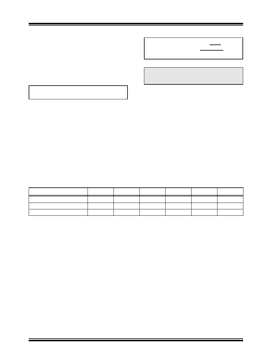
TABLE 15-2:
EXAMPLE PWM FREQUENCIES AND RESOLUTIONS AT 40 MHz
PWM Duty Cycle = (CCPR1L:CCP1CON<5:4>)
TOSC (TMR2 Prescale Value)
Note:
If the PWM duty cycle value is longer than
the PWM period, the CCP1 pin will not be
cleared.
(
)
PWM Resolution (max) =
FOSC
FPWM
log
log(2)
bits
PWM Frequency
2.44 kHz
9.77 kHz
39.06 kHz
156.25 kHz
312.50 kHz
416.67 kHz
Timer Prescaler (1, 4, 16)
16
41111
PR2 Value
FFh
3Fh
1Fh
17h
Maximum Resolution (bits)
10
8
7
6.58
发布紧急采购,3分钟左右您将得到回复。
相关PDF资料
PIC18F4410-E/PT
IC MCU FLASH 8KX16 44TQFP
PIC24F16KL401-I/SS
IC MCU 16BIT 16KB FLASH 20-SSOP
PIC24F08KL402-I/SO
IC MCU 16BIT 8KB FLASH 28-SOIC
PIC16F690-I/SO
IC PIC MCU FLASH 4KX14 20SOIC
PIC24F08KL201-I/SO
IC MCU 16BIT 8KB FLASH 20-SOIC
PIC18F4331-E/ML
IC MCU FLASH 4KX16 44QFN
PIC16C622A-04/P
IC MCU OTP 2KX14 COMP 18DIP
PIC16F1936-I/ML
IC PIC MCU FLASH 512KX14 28-QFN
相关代理商/技术参数
PIC18F4410T-I/PT
功能描述:8位微控制器 -MCU 16KB 768 RAM 36I/O RoHS:否 制造商:Silicon Labs 核心:8051 处理器系列:C8051F39x 数据总线宽度:8 bit 最大时钟频率:50 MHz 程序存储器大小:16 KB 数据 RAM 大小:1 KB 片上 ADC:Yes 工作电源电压:1.8 V to 3.6 V 工作温度范围:- 40 C to + 105 C 封装 / 箱体:QFN-20 安装风格:SMD/SMT
PIC18F4420-E/ML
功能描述:8位微控制器 -MCU 16KB 768 RAM 36I/O RoHS:否 制造商:Silicon Labs 核心:8051 处理器系列:C8051F39x 数据总线宽度:8 bit 最大时钟频率:50 MHz 程序存储器大小:16 KB 数据 RAM 大小:1 KB 片上 ADC:Yes 工作电源电压:1.8 V to 3.6 V 工作温度范围:- 40 C to + 105 C 封装 / 箱体:QFN-20 安装风格:SMD/SMT
PIC18F4420-E/P
功能描述:8位微控制器 -MCU 16KB 768 RAM 36I/O RoHS:否 制造商:Silicon Labs 核心:8051 处理器系列:C8051F39x 数据总线宽度:8 bit 最大时钟频率:50 MHz 程序存储器大小:16 KB 数据 RAM 大小:1 KB 片上 ADC:Yes 工作电源电压:1.8 V to 3.6 V 工作温度范围:- 40 C to + 105 C 封装 / 箱体:QFN-20 安装风格:SMD/SMT
PIC18F4420-E/PT
功能描述:8位微控制器 -MCU 16KB 768 RAM 36I/O RoHS:否 制造商:Silicon Labs 核心:8051 处理器系列:C8051F39x 数据总线宽度:8 bit 最大时钟频率:50 MHz 程序存储器大小:16 KB 数据 RAM 大小:1 KB 片上 ADC:Yes 工作电源电压:1.8 V to 3.6 V 工作温度范围:- 40 C to + 105 C 封装 / 箱体:QFN-20 安装风格:SMD/SMT
PIC18F4420-I/ML
功能描述:8位微控制器 -MCU 16KB 768 RAM 36I/O RoHS:否 制造商:Silicon Labs 核心:8051 处理器系列:C8051F39x 数据总线宽度:8 bit 最大时钟频率:50 MHz 程序存储器大小:16 KB 数据 RAM 大小:1 KB 片上 ADC:Yes 工作电源电压:1.8 V to 3.6 V 工作温度范围:- 40 C to + 105 C 封装 / 箱体:QFN-20 安装风格:SMD/SMT
PIC18F4420-I/P
功能描述:8位微控制器 -MCU 16KB 768 RAM 36I/O RoHS:否 制造商:Silicon Labs 核心:8051 处理器系列:C8051F39x 数据总线宽度:8 bit 最大时钟频率:50 MHz 程序存储器大小:16 KB 数据 RAM 大小:1 KB 片上 ADC:Yes 工作电源电压:1.8 V to 3.6 V 工作温度范围:- 40 C to + 105 C 封装 / 箱体:QFN-20 安装风格:SMD/SMT
PIC18F4420-I/PT
功能描述:8位微控制器 -MCU 16KB 768 RAM 36I/O RoHS:否 制造商:Silicon Labs 核心:8051 处理器系列:C8051F39x 数据总线宽度:8 bit 最大时钟频率:50 MHz 程序存储器大小:16 KB 数据 RAM 大小:1 KB 片上 ADC:Yes 工作电源电压:1.8 V to 3.6 V 工作温度范围:- 40 C to + 105 C 封装 / 箱体:QFN-20 安装风格:SMD/SMT
PIC18F4420T-I/ML
功能描述:8位微控制器 -MCU 16KB 768 RAM 36I/O RoHS:否 制造商:Silicon Labs 核心:8051 处理器系列:C8051F39x 数据总线宽度:8 bit 最大时钟频率:50 MHz 程序存储器大小:16 KB 数据 RAM 大小:1 KB 片上 ADC:Yes 工作电源电压:1.8 V to 3.6 V 工作温度范围:- 40 C to + 105 C 封装 / 箱体:QFN-20 安装风格:SMD/SMT